-
Mail us
contact@tiger-transformer.com -
Phone us
(+86)15655168738 -

Mail us
contact@tiger-transformer.comPhone us
(+86)15655168738
When the design needs to prioritize and reduce EMI (electromagnetic interference) as much as possible, linear voltage regulators can be regarded as a low-noise solution, but considering the heat dissipation and efficiency requirements, they are not suitable for this scenario. Instead, you need to choose a switching regulator. Even in EMI-sensitive applications, the switching regulator is often the first active component on the input power bus, which can significantly affect the overall converter's EMI performance regardless of the downstream converter. Make sure that you can suppress EMI and meet efficiency requirements through the selection of power IC. The LT8614 Silent Switcher regulator does this.
The LT8614 reduces EMI by more than 20dB compared to current switching regulators. In contrast, it reduces EMI by a factor of 10 in the frequency range above 30MHz without compromising minimum turn-on and turn-off times or efficiency in equivalent circuit board area. It achieves this without additional components or shielding, representing a major breakthrough in switching regulator design.
New solutions to improve EMI problems
A reliable way to solve EMI (electromagnetic interference) problems is to use a shielding box for the entire circuit. Of course, this significantly increases the required board space, components, and assembly costs, while increasing the complexity of thermal management and testing. Another approach is to slow down the edge of the switch. However, this can have the undesirable effects of reduced efficiency, increased minimum on and off times and their associated dead times, and affects potential potential current control loop speed.
The LT8614 Silent Switcher regulator achieves the desired effect without using a shielding box (see Figure 1). The LT8614 has an IQ as low as 2.5µA, and when regulated with no load, the device consumes a total supply current of 2.5µA, which is important in always-on systems.
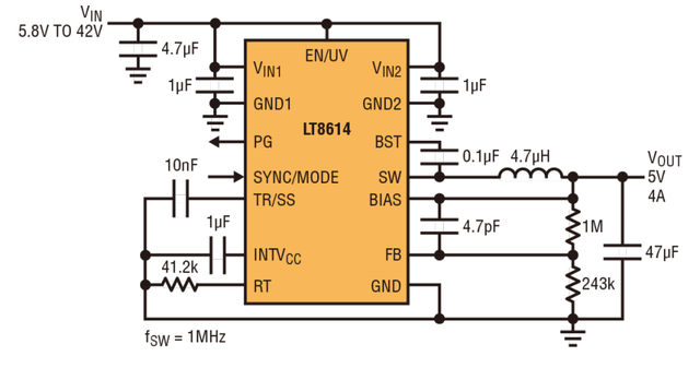
Figure 1. LT8614 Silent Switcher can fully reduce EMI/EMC radiation while achieving high efficiency (conversion) at frequencies up to 3MHz.
The ultra-low dropout voltage is limited only by the internal top switch. Unlike other solutions, the LT8614's VIN-VOUT (input and output voltage) limits are not limited by the maximum duty cycle and minimum off-time. As shown in Figure 6, the device skips the shutdown period when a voltage drop occurs to keep the internal top-switching boost stage voltage stable.
At the same time, the typical minimum operating input voltage is only 2.9V (maximum 3.4V), allowing it to provide a voltage of 3.3V in a buck state. Because the total switching resistance of LT8614 is low, its efficiency is higher than similar devices under high current conditions.
The LT8614 (operating frequency) can be synchronized with an external operating frequency from 200kHz to 3MHz. Since AC switching losses are lower, it can operate at high switching frequencies with minimal losses. A good balance is achieved in EMI-sensitive applications such as those common in many automotive environments, and the LT8614 can operate below the AM band to achieve lower EMI, or it can operate above the AM band. In a setup with an operating switching frequency of 700kHz, the standard LT8614 demo board did not exceed the noise floor in any of the CISPR25 Level 5 measurements.
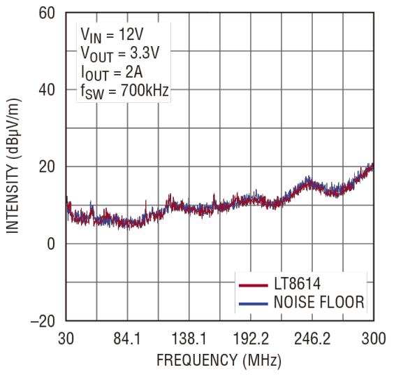
Figure 2. LT8614 board complies with CISPR25 radiation in an anechoic chamber standard. The noise floor is comparable to the electromagnetic radiation disturbance of the LT8614.
Figure 2 shows the results of measurements in an anechoic chamber with an input voltage of 12V, an output voltage of 3.3V, a current of 2A, and a fixed switching frequency of 700kHz. To compare the LT8614 to another switching regulator, this product was measured against the LT8610 (see Figure 3). In the GTEM chamber, standard demonstration boards for both devices were tested using the same load, input voltage, and the same inductance.
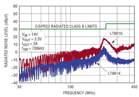
Figure 3. Comparison of electromagnetic radiation disturbance between LT8614 and LT8610 .
It can be found that compared with the already good EMI performance of LT8610, using LT8614 can improve it by another 20dB, especially in the more difficult to manage high frequency range.
In the time domain, the LT8614 performs well at the edge of the switch node, as shown in Figures 4 and 5. Even at 4ns/div, the LT8614 regulator has very little ringing. As shown in Figure 4, the LT8610 has good ringing rejection in comparison, but it can be seen to store more energy in the hot loop compared to the LT8614 (Figure 4).
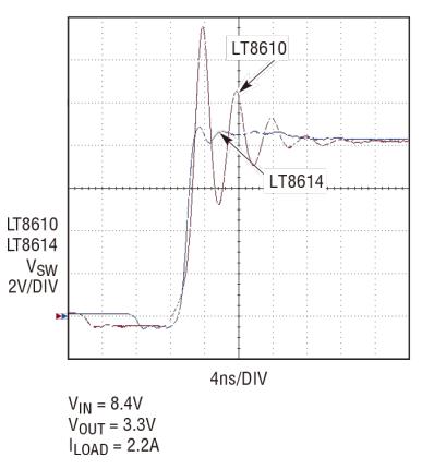
Figure 4. Switch node rise of LT8614 Silent Switcher and LT8610 Comparison along the edges.
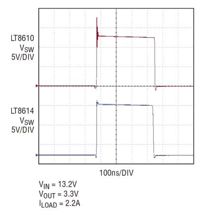
Figure 5. LT8614 nearly ideal square wave switching waveform implementation for low noise operation.
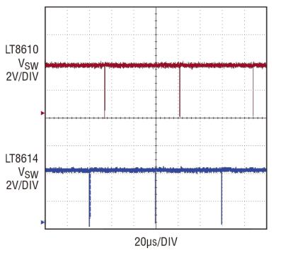
Figure 6. Voltage drop of switch node of LT8614 and LT8610 performance.
Figure 5 shows the switching node at a 13.2V input voltage and how the LT8614 achieves a near-ideal square wave at the switching node. All time domain measurements in Figures 4, 5, and 6 were made using a 500MHz Tektronix P6139A probe with the probe tip shield tightly connected to the GND plane of the PCB. Both devices use off-the-shelf demonstration boards.
The LT861x family has an absolute maximum input voltage rating of 42V, which is important for automotive and industrial environments. In automotive applications, voltage drop performance is as important as its (maximum input voltage rating). Typically, the critical 3.3V logic supply must be supported during cold boot conditions. In this case, the LT8614 Silent Switcher regulator maintains the near-ideal performance of the LT861x series. As shown in Figure 6, instead of using the higher undervoltage lockout voltage and maximum duty cycle clamping features of the alternative parts, the LT8610/11/14 devices operate down to 3.4V and begin skipping cycles when necessary. This results in ideal pressure drop performance.
The LT8614 has a minimum on-time of 30ns, enabling a large step-down ratio even at high switching frequencies. Therefore, it can provide the logic core voltage with a single step-down at input voltages up to 42V.
Conclusion
As we all know, in order to pass the electromagnetic interference test when the system design is completed, the electromagnetic interference problem needs to be carefully considered during the initial design stage of the converter. The LT8614 voltage regulator can ensure the successful and feasible realization of this requirement through the selection of power ICs. The LT8614 reduces the electromagnetic interference generated by current advanced switching regulators by more than 20dB, and does not require additional components or additional shielding even if the conversion efficiency is improved.
Switching Regulators and EMI
Printed circuit board layout design determines the functionality, electromagnetic interference, and thermal behavior of a power supply and determines the success or failure of every power supply design. Although the layout of a switching power supply is not magic, it is often overlooked during the initial design process. Since functional and electromagnetic interference requirements must be met, factors that favor the functional stability of the power supply usually also favor electromagnetic interference emissions. Know that having a good layout from the beginning not only does not increase costs, it actually saves costs and eliminates the need to change EMI filters, mechanical shielding, EMI test time, and PC boards.
There are two types of EMI emissions: conducted and radiated. Conducted emissions are connected to the product through wires and traces. Because this noise is localized to specific terminals or connectors in the design, compliance with conducted emissions requirements can usually be guaranteed early in the development process through good layout and filter design.
Radiated emissions, however, are another story. Anything on a circuit board that carries electrical current will radiate electromagnetic fields. Every trace on the board is an antenna, and every copper layer is a mirror. Anything other than a pure sine wave or DC voltage will produce a wider signal spectrum. Even with careful design, developers have no way of truly knowing how serious a radiated emission situation will be until the system is tested. Radiated emission testing can only be formally carried out after the design is basically completed.
Filters usually reduce electromagnetic interference by attenuating signal strength at a certain frequency or within a certain frequency range. By adding metal plates as magnetic shields, some of the energy in space (radiation) can be attenuated. Suppress energy in the low frequency portion of the PCB traces (conduction) by adding ferrite beads and other filters. EMI cannot be eliminated, but it can be attenuated to a level acceptable to other communications and digital devices. In addition, some regulatory agencies ensure compliance by implementing relevant standards.
Modern input filters using surface mount technology have better performance than through-hole devices. However, this improvement has not kept pace with increases in switching regulator operating frequencies. Higher efficiency, shorter on and off times, and faster switching transitions result in higher harmonic content. When all other parameters (such as switching capacity and switching time) are held constant, EMI worsens by 6dB every time the switching frequency is doubled. If the switching frequency is increased by a factor of 10, the broadband EMI performance will be like a first-order high-pass filter, with a 20dB increase in radiation.
Savvy PCB designers will keep thermal loops small and keep the shielded ground plane as close to the active layer as possible. Nonetheless, device pinout, package construction, thermal design requirements, and package size required to store sufficient energy in the decoupling components all dictate that thermal loops be kept as small as possible. To further complicate matters in a typical flat PCB design, magnetic or transformer-like coupling between traces above 30MHz will weaken all filters since bad magnetic coupling or antenna coupling becomes more significant at higher frequencies. effect.
Potential interference and noise problems may become more severe when multiple DC/DC switch-mode regulators are connected in parallel to achieve current sharing and higher output power. If all regulators operate (switch) at a similar frequency, then the combined energy produced by multiple regulators in the circuit will be concentrated at that frequency and its harmonics. The presence of this energy can be a difficult problem for other ICs on the PC board and other system boards, where devices are in close proximity and susceptible to this radiated energy. This problem is particularly worrisome in automotive systems, where components are densely packed and often in close proximity to audio, radio frequency, CAN buses, and various receiving systems.
