-
Mail us
contact@tiger-transformer.com -
Phone us
(+86)15655168738 -

Mail us
contact@tiger-transformer.comPhone us
(+86)15655168738
Traditional Y capacitors are mainly in the form of plug-ins. Since Keya launched the JK-ET series of chip Y capacitors, many people have been confused about what the internal structure of chip Y capacitors looks like. How is it different from traditional plug-in Y capacitors? What's the difference?
In order to let everyone see the internal structure of the chip Y capacitor more intuitively, we have drawn a simple diagram for you, as shown below:
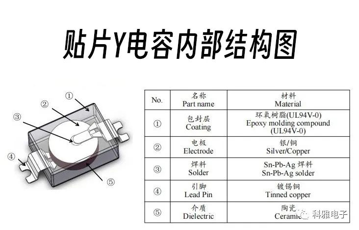
It can be seen that whether it is a plug-in Y capacitor or a chip Y capacitor, Their internal chips are exactly the same, but the external packaging methods are obviously different. Relatively speaking, the external packaging method of SMD Y capacitors is more complicated.
Relatively speaking, the reliability of SMD Y capacitors with respect to moisture and heat has been improved. For example, the Keya JK-ET series plastic-encapsulated SMD Y1-cap can meet the PCT requirements of 121°C, 2atm., 100%RH, and 24h. Experimental requirements, while traditional plug-in Y capacitors cannot meet this requirement.
However, due to the small size of the chip Y capacitor, the capacity of the Y capacitor that cannot be made is generally not too large, and the large-capacity Y capacitor must be in the form of a plug-in.
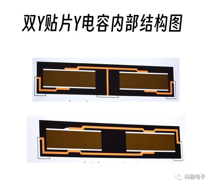
In addition to single-chip SMD Y capacitors, Keya also launched dual-chip SMD Y capacitors, one of which can replace two Y capacitors. The internal structure diagram is as follows:
The role of SMD Y capacitor:
The most ideal use is as AC line filter and primary and secondary coupling of switching power supplies and AC adapters.
The most ideal use is DA isolation and noise reduction for transformerless DAA modems.
Mount capacitors on the PCB surface to increase PCB space utilization.
Products with rated voltages of AC250V & AC400V are available.
