-
Mail us
contact@tiger-transformer.com -
Phone us
(+86)15655168738 -

Mail us
contact@tiger-transformer.comPhone us
(+86)15655168738
Combined with the schematic diagram, I try to explain the switching waveforms of the voltage and current at each key point of the flyback switching power supply in the steady state of the discontinuous mode DCM, without involving the specific component parameter values.
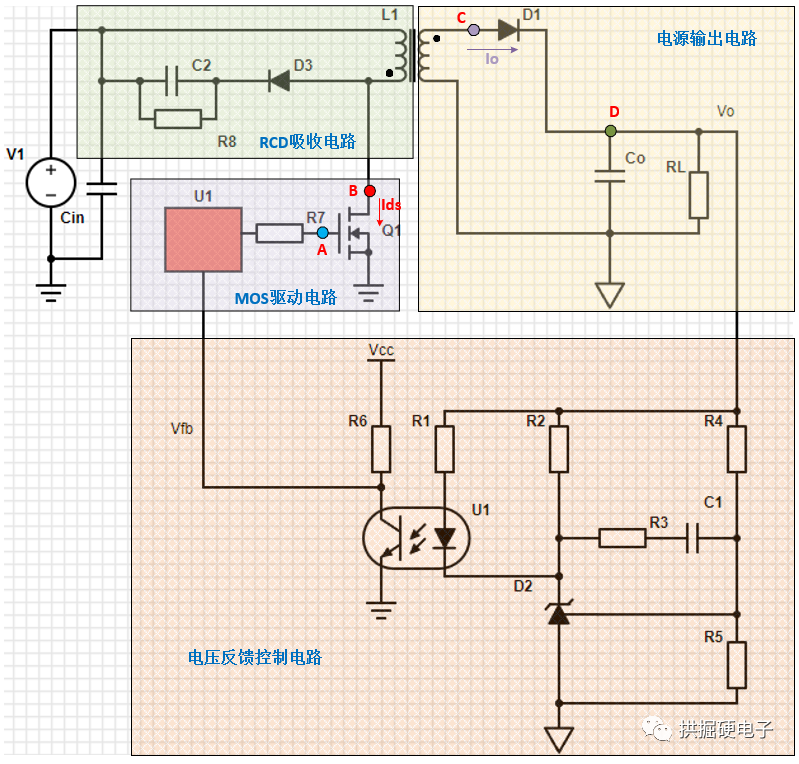
Basic working principle of flyback switching power supply
When the MOS transistor Q1 is turned on, the primary winding of the transformer L1 is charged. When the MOS tube is turned off, the energy stored in the primary winding is transferred to the secondary winding.
The flyback switching power supply mainly includes a power input circuit, a MOS drive circuit, an RCD absorption circuit, a power output circuit, and a voltage feedback control circuit. Other circuits that may be used in switching power supplies, such as current sampling protection circuits, power startup circuits, and slope compensation circuits, will not be discussed in this article.
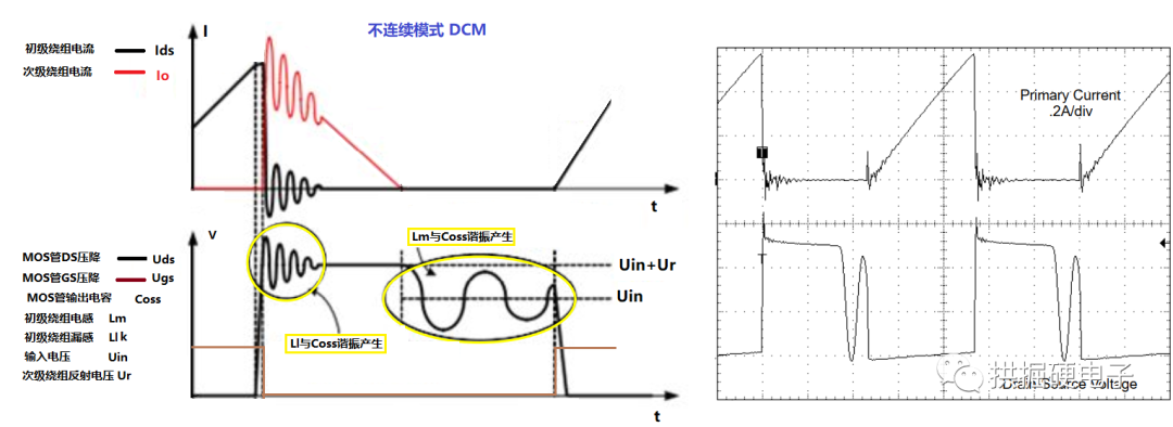
MOS tube drive circuit waveform
The left figure is a schematic diagram of the relevant waveforms of the MOS tube drive circuit (current discontinuous mode DCM), where Uin corresponds to V1 in the above figure, and Ugs corresponds to the voltage waveform at point A in the above figure. The figure on the right is the measured waveform of a flyback switching power supply, which only reflects the primary winding current and MOS tube DS voltage drop.
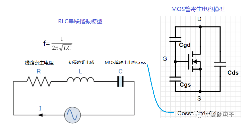
The Uds waveform in the left figure has two oscillation waveforms, which are respectively generated by the resonance of the primary winding leakage inductance Llk and the parasitic capacitance Coss of the MOS tube, and are generated by the resonance of the primary winding inductance Lm and the parasitic capacitance Coss of the MOS tube. Since the primary winding leakage inductance Llk is much smaller than the primary winding inductance Lm, for example, the former is 1%~5% of the latter, so the frequency of the first resonant waveform is much higher than that of the second. The first voltage resonance waveform gradually returns to a stable state, and the Uds voltage amplitude is the secondary reflected voltage at this time. When the second resonance starts, the MOS tube is in the off state, the output diode is in the off state, and the secondary winding current is zero.
In this circuit, the series resonant inductor and capacitor The basic model is as follows. At the resonant frequency, the impedances of the inductor and the capacitor cancel each other out, and there is only the parasitic resistance of the line in the entire loop.
The inductor charges the capacitor, and then the capacitor charges the inductor. The energy circulates between the two, and the energy Difficult to consume, a resonant voltage waveform is formed.
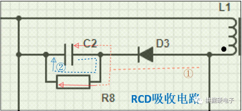
RCD absorption circuit waveform
When the MOS is turned off, the function of the RCD absorption circuit is to absorb the voltage spikes at both ends of the MOS transistor DS, preventing the D pole of the MOS transistor from being damaged by the Uds voltage spike breakdown or affecting the service life of the MOS transistor.
Uc represents the voltage across the clamping capacitor C2, and its voltage should not exceed the design value of the Uclamp clamping voltage (the forward conduction voltage drop of the diode has been ignored), so that Uclamp+Uin<80%× MOS tube DS withstand voltage. Note that the V-axis amplitude in the figure on the right does not start from 0V, but from Uin.
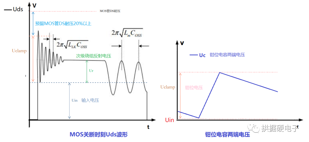
Uds voltage waveform (red) and Uclamp of a switching power supply The voltage waveform (blue) is as follows:

When the voltage When it rises, it corresponds to the initial moment when the MOS tube is turned off. At this moment, the Uds voltage peak charges the capacitor C2 through the diode D3, as shown in the current path ① in the figure below. When the Uds voltage peak is smaller than the capacitor voltage, the diode D3 is cut off, and the capacitor C2 discharges to the resistor, see the current path ②.
Power output circuit waveform
When the power supply is in a steady state, at the time ton, the MOS tube is turned on, the inductance current of the primary winding increases linearly, and the capacitor Co supplies power to the load RL, see the path of the capacitor discharge current Ic1 in the figure below. Because the non-inverting terminals of the primary winding and the side winding of the transformer used in the flyback switching power supply are opposite. At time ton, the primary winding suppresses the increase of the current, the induced voltage of the primary winding is positive and negative, the induced voltage of the side winding Lp is negative and positive, and the diode D1 is in the cut-off state.
At the toff moment, the MOS is turned off, the energy stored in the primary winding is transmitted to the secondary winding, the primary winding maintains the original current direction, the induced voltage of the primary winding is negative and positive, and the induced voltage of the secondary winding Positive and negative, the diode D1 is in the conduction state, and the secondary winding supplies power to the capacitor Co and the load RL through the diode D1.
The lower right figure is the actual measurement result of the output voltage ripple voltage of a switching power supply. Therefore, at time ton, the voltage waveform time at both ends of the capacitor Co corresponds to the current discharge time of Ic1. At the moment toff, the voltage waveform time at both ends of the capacitor Co corresponds to the charging time of the Ic2 current.

Voltage feedback control circuit waveform
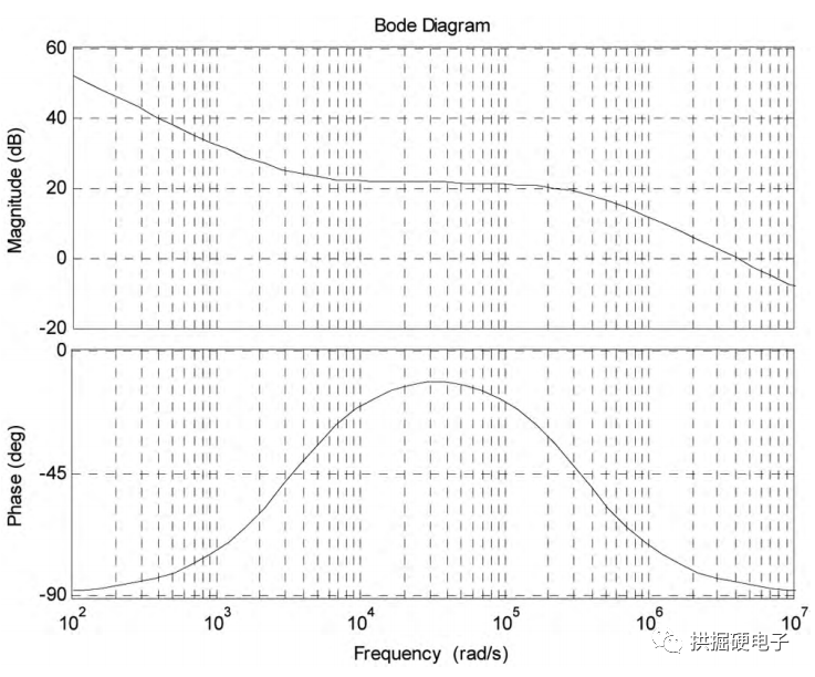
In this part of the circuit, the Bode diagram of the transfer function of the open-loop system is usually used, combined with the stability criterion of the Bode diagram to discuss and judge the stability of the switching power supply.
Sufficient amplitude margin and phase margin are necessary, otherwise the dynamic response characteristics of the switching power supply system are relatively poor, or the output voltage will oscillate.
The figure below is the Bode diagram of the switching power supply voltage control frequency compensation loop transfer function, the phase margin is greater than 90°, the low frequency gain is 40 dB, and the intermediate frequency gain is 20dB. After actual measurement, the output voltage is stable. Good dynamic response characteristics.